(China (Mainland))

Product Summary
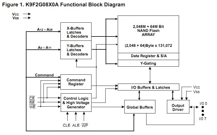
The K9F2G08UOA-PCBO is a 2G-bit NAND Flash Memory with spare 64M-bit. Its NAND cell provides the most cost-effective solution for the solid state application market. A program operation can be performed in typical 200µs on the (2K+64)Byte page and an erase operation can be performed in typical 1.5ms on a (128K+4K)Byte block. The K9F2G08UOA-PCBO on-chip write controller automates all program and erase functions including pulse repetition, where required, and internal verification and margining of data. Even the write-intensive systems can take advantage of the K9F2G08UOA-PCBO’s extended reliability of 100K program/erase cycles by providing ECC(Error Correcting Code) with real time mapping-out algorithm. The K9F2G08UOA-PCBO is an optimum solution for large nonvolatile storage applications such as solid state file storage and other portable applications requiring non-volatility.
Parametrics
K9F2G08UOA-PCBO absolute maximum ratings: (1)Voltage on any pin relative to VSS, VCC: -0.6 to +2.45V; VIN: -0.6 to +2.45V; VI/O: -0.6 to Vcc + 0.3V; (2)Temperature Under Bias, TBIAS: -10 to +125℃; (3)Storage Temperature, TSTG: -65 to +150℃; (4)Short Circuit Current, IOS: 5 mA.
Features
K9F2G08UOA-PCBO features: (1)Voltage Supply: 1.65V to 1.95V; 2.70V to 3.60V; (2)Organization: Memory Cell Array: (256M + 8M) x 8bit; Data Register: (2K + 64) x 8bit ; (3)Automatic Program and Erase: Page Program: (2K + 64)Byte; Block Erase: (128K + 4K)Byte; (4)Page Read Operation: Page Size: (2K + 64)Byte; Random Read: 25μs(Max.); Serial Access: 25ns(Min.).
Diagrams
 |
 K9F2808Q0B-D |
Other |
|
Data Sheet |
Negotiable |
|
||||
|
K9F2808Q0C-DCB0 |
Other |
|
Data Sheet |
Negotiable |
|
||||
|
K9F2808U0A-YCB0 |
Other |
|
Data Sheet |
Negotiable |
|
||||
|
K9F2808U0A-YIB0 |
Other |
|
Data Sheet |
Negotiable |
|
||||
|
K9F2808U0B-D |
Other |
|
Data Sheet |
Negotiable |
|
||||
|
K9F2808U0B-V |
Other |
|
Data Sheet |
Negotiable |
|
||||